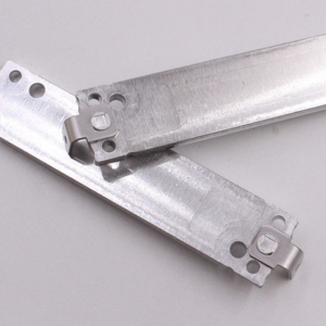


Overview
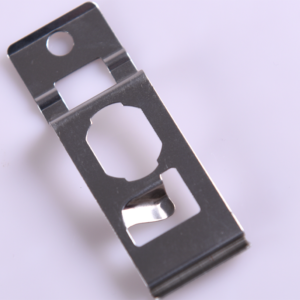
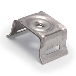
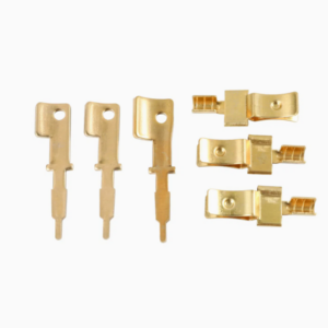
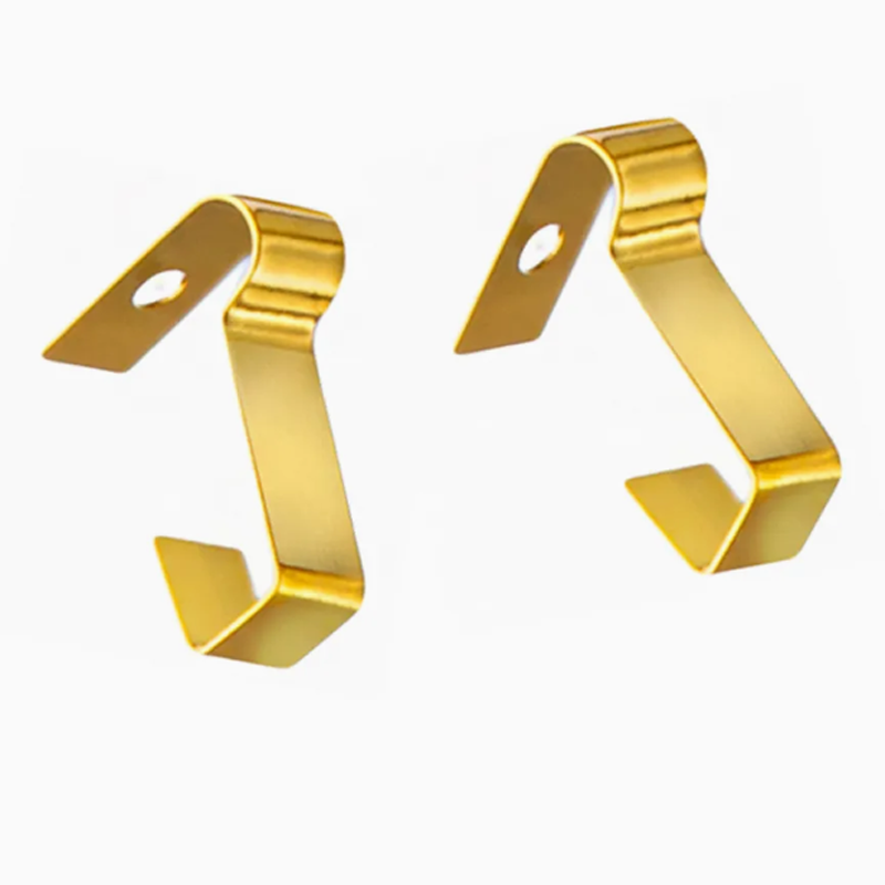
Our custom progressive stamping shrapnel contacts for PCB boards are precision-engineered to ensure reliable electrical connectivity in compact electronics. Manufactured from high-performance copper alloys via advanced multi-stage progressive dies, they offer exceptional spring force, conductivity, and long-term durability. We provide comprehensive OEM services, including material selection, plating, and precise forming to meet your exact electrical and mechanical specifications.
Features
| Attribute | Details |
|---|---|
| Product Name | PCB Shrapnel / Spring Contact |
| Primary Material | C5191, C5210, C17200, C7541 (CuSn, CuNiSn, BeCu) |
| Processing Type | High-Speed Progressive Stamping |
| Material Thickness | 0.05mm – 0.3mm (Typical) |
| Mould | Multistep Progressive Dies (Precision Hardened) |
| Surface Processing | Selective Plating (Gold, Tin, Silver, Nickel) |
| Process | Forming, Coining, Bending |
| Industry | Consumer Electronics, Automotive Electronics, Connectors |
| Tolerances | ±0.02mm (Critical Contact Areas) |
| Customized | Yes (Design to Spec) |
| Transport Package | Tape & Reel, Anti-Tarnish Packaging, Custom Carrier |
| Trademark | OEM |
| Origin | Xiamen, China |
| Production Capacity | High-Volume (Project Based) |
The Advantages of Our PCB Shrapnel Contacts
-
Ultra-Precise Forming & Tolerance Control: Our progressive dies and coining processes achieve dimensional tolerances within ±0.02mm, ensuring consistent contact height, mating force, and precise alignment for automated PCB assembly (SMT/PTH).
-
Engineered for Optimal Electrical & Mechanical Performance: We select and process materials like phosphor bronze and beryllium copper to deliver the perfect balance of high conductivity, necessary spring hardness (HV), and excellent fatigue resistance for millions of cycles.
-
Burr-Free & Clean Edge Finish: Advanced fine-blanking techniques within the progressive die and precise deburring post-processing guarantee smooth, flash-free edges. This prevents short circuits and ensures reliable solderability or press-fit performance.
-
Integrated Design & Full Finishing Services: We offer end-to-end solutions from DFM to delivery, including in-house selective electroplating (e.g., gold on contact tip, tin on solder tail) to enhance conductivity, corrosion resistance, and solderability as per your requirements.
Production Process
-
Material Selection & Slitting: High-grade copper alloy strip is selected based on required conductivity, springback, and hardness. It is precision-slitted to the exact width for the progressive die.
-
Precision Progressive Die Stamping: The coil is fed through a multi-station progressive die where operations like piloting, blanking, forming, coining (for contact surface), and final cut-off are performed in one continuous, high-speed operation.
-
Secondary Forming & Heat Treatment: For complex 3D shapes, a secondary forming or bending operation may follow. Heat treatment (age hardening) is applied to beryllium copper and other alloys to achieve the specified spring temper and hardness.
-
Surface Finishing & Plating: Contacts undergo cleaning and selective electroplating (e.g., Au over Ni, matte Sn) on designated areas to ensure reliable electrical contact and corrosion protection. Anti-tarnish coatings may be applied.
-
Comprehensive Quality Inspection: 100% automated optical inspection (AOI) checks for dimensional accuracy and defects. Sample testing verifies critical parameters: contact force (via force gauge), electrical resistance, and solderability.
-
Packaging: Finished contacts are packaged using tape-and-reel, blister trays, or custom carriers compatible with high-speed automated placement equipment to prevent damage and oxidation.
Our Factory
Our facility is equipped for high-precision, high-volume stamping of micro-components. We operate a battery of high-speed precision progressive stamping presses (25T to 150T) and maintain an in-house tool & die workshop with CNC, Wire-EDM, and grinding centers for crafting and maintaining precision dies. Our integrated plating shop supports reel-to-reel selective plating processes. Quality is assured through a dedicated metrology lab featuring non-contact optical measuring systems and advanced testing equipment for material and electrical properties. This vertically integrated setup, under strict quality protocols, enables us to deliver reliable, complex shrapnel contacts for the global electronics industry.